Future concepts
Division
Building on a legacy of breakthrough innovations
In 2023, the Palo Alto Research Center (PARC) joined SRI, bringing together two iconic Silicon Valley research organizations to build, expand, and scale capabilities, and offer an even more diverse technology set for our government and commercial customers. It formed the foundation for SRI’s sixth division – the Future Concepts division. With expertise across numerous areas, including developing solutions for a more sustainable world and creating a digital future for the workplace, the division puts a premium on developing integrated concepts for complex problems and driving and catalyzing collaboration across SRI. The labs in the Future Concepts division focus on basic research and real-world applications by creating and maturing breakthrough technologies.
80+ Researchers across two labs
50+ Years of extraordinary innovations
50+Projects in 2023

“As a division within SRI, we deliver solutions across a wide range of technologies, especially as we grapple with global issues like climate and energy. We are a passionate group of scientists and engineers with a solid track record of innovation in creating new technologies and bringing them to the world for the benefit of humanity.”
Jan VandenbrandeSenior Vice President, Future Concepts division
Find out about our labs
Real-world impact
-
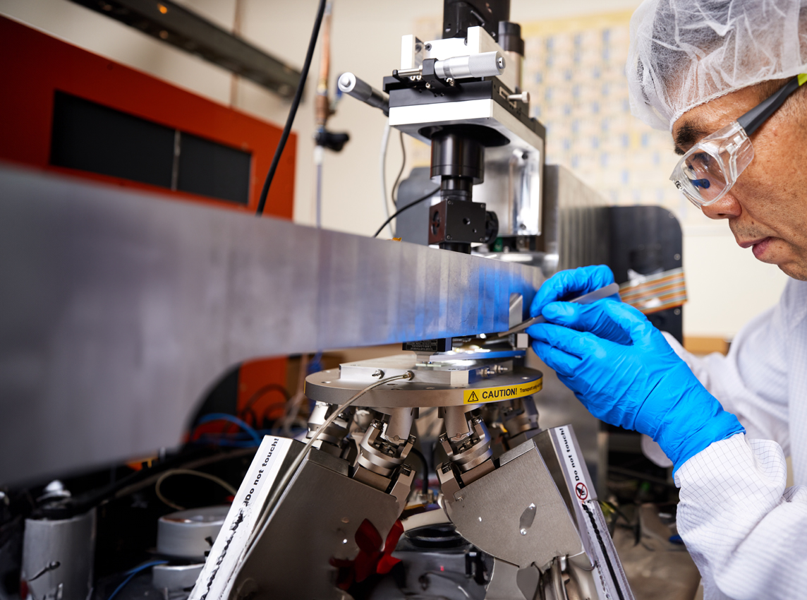
Researchers aim to disrupt how new materials are leveraged in the design process
SRI chosen by DARPA to develop next-generation computational design of metallic parts and intelligent testing of alloys.
-
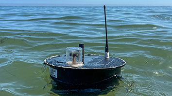
SRI researchers develop rugged, low-cost, drifting sensors to learn more about the oceans
PEARL drifters pack an array of sensors into a compact autonomous device to gather data and signs of activity.
-
SRI Honors Women’s Progress: Paying Tribute to Women’s History Month
We foster environments where women can innovate, lead, and contribute.